🏢 Facility Overview
The i-BRAIN Nanofabrication Facility features 550 m² of Class 100 cleanroom space and 400 m² of Class 1000 service and equipment areas, supporting research and prototyping on wafers up to 200 mm (8 inches). The facility is equipped for advanced lithography, including electron-beam lithography, DUV scanner, mask aligners, maskless aligners, automatic coater/developer tracks, spin coaters, and hotplates. Thin-film deposition capabilities include e-beam evaporators for metals and sputtering systems for metal oxides. Etching tools include wet benches and plasma ashers, while metrology and characterization are supported by CD-SEM, optical microscopes, and profilometers. The facility provides a comprehensive environment for micro- and nanofabrication, enabling cutting-edge research and device development.
Lithography Bay
The Lithography Bay is a core area of the i-BRAIN Nanofabrication Facility, dedicated to high-precision patterning of micro- and nanoscale structures on wafers up to 200 mm (8 inches).
It houses state-of-the-art lithography tools:
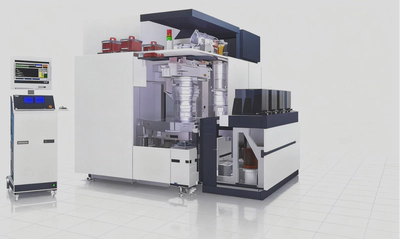
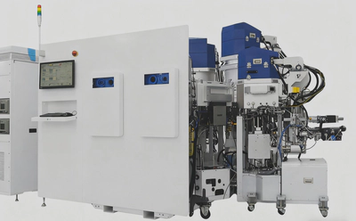
ASML KrF Stepper: Deep-UV projection lithography down to 110 nm resolution on 200 mm wafers.
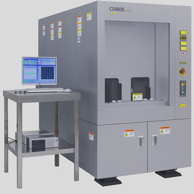
Electron-Beam Lithography (EBL) System: 50 kV operation for high-resolution patterning on wafers up to 200 mm.
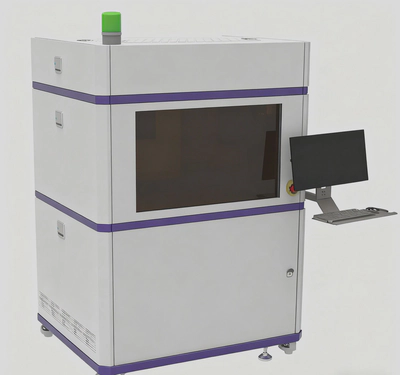
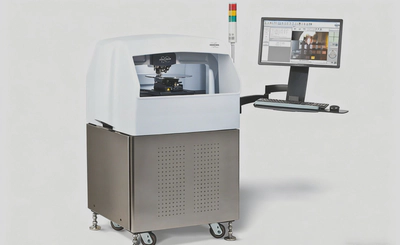
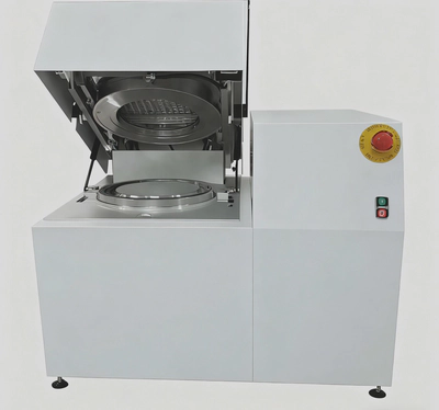
Maskless Aligner: Up to 300 mm wafer size, reticle resolution 600 nm, ideal for flexible and rapid prototyping.
Mask Aligner: Exposure area up to 210 × 210 mm, equipped with 365 nm, 405 nm, and 435 nm light sources for contact and proximity lithography.
Supporting Equipment: Automated coater/developer tracks, spin coaters, and hotplates for full resist application and baking workflows.
Deposition Bay
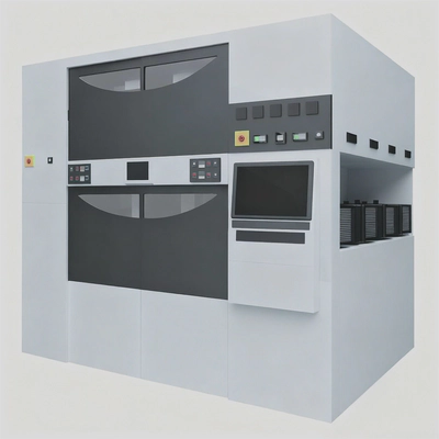
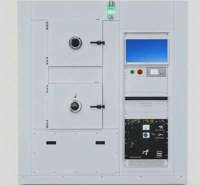
The Deposition Bay provides advanced thin-film deposition capabilities for metals and metal oxides, supporting device fabrication on wafers up to 200 mm. Key equipment includes:
Electron-Beam Evaporators: High-purity deposition of metals such as Au, Pt, Ti, Cr, Ni, and others with precise thickness control.
Sputtering System: Deposition of metal oxide films for functional layers in micro/nano devices.
Metrology & Other Bay
The Metrology & Other Bay provides comprehensive measurement, inspection, and processing capabilities to ensure precise fabrication and process control. Key tools and capabilities include:
CD-SEM: High-resolution critical dimension measurement for nanoscale patterns.
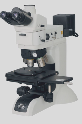
Optical Microscopes: Inspection and alignment verification across wafer surfaces.
Profilometers: Surface topography and film thickness measurements for thin films and patterned structures.
Rapid Thermal Processing (RTP): Controlled heating for annealing, curing, and other thermal treatments.
O₂ Plasma Asher: Surface treatment and photoresist removal using oxygen plasma for cleaning and pattern definition.